Five-Day IEP on ASIC Design Successfully Concluded!
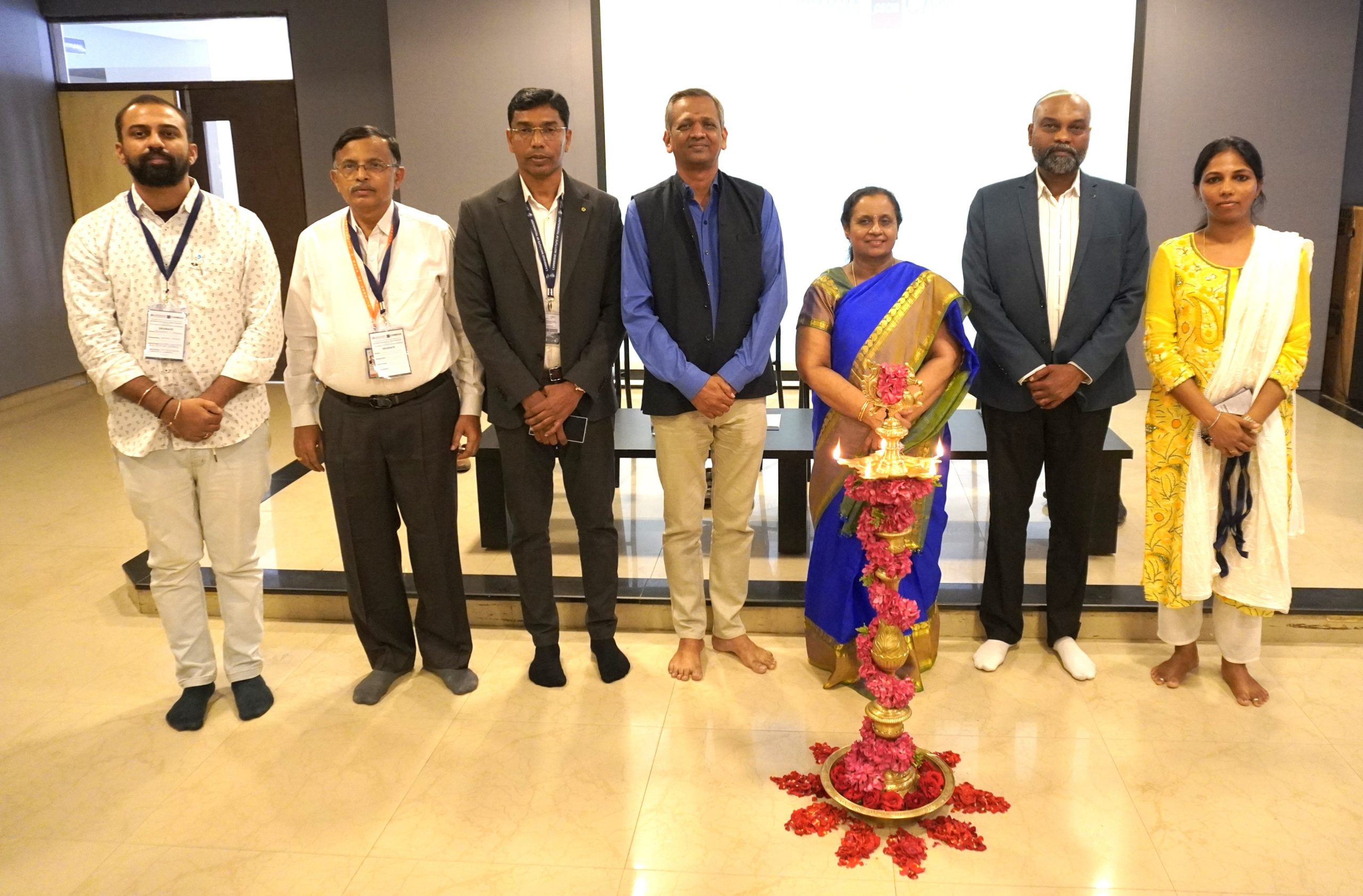
The Department of Electronics and Communication Engineering (ECE), Cambridge Institute of Technology (CIT), successfully organized a Five-Day Instruction Enhancement Program from 23rd to 27th February 2026 on “ASIC Design Flow Using SCL 180nm Technology,” featuring an in-depth case study on a Dual 8-Point FFT Processor with Bus Interfaces. Conducted under the aegis of CCCIR (Centre for Collaborative and Corporate Industry Relations) and supported by the Ministry of Electronics and Information Technology (MeitY), Government of India, the Chips to Startup (C2S) Programme, and the Centre for Development of Advanced Computing (C-DAC), the program was designed to strengthen academic expertise and practical competency in VLSI and ASIC design. The sessions provided comprehensive exposure to the complete ASIC design lifecycle, including system specification, RTL design, simulation, synthesis, timing analysis, physical design, verification, and layout validation using SCL 180nm technology, one of India’s significant semiconductor fabrication platforms. The featured case study enabled participants to understand the architectural design and integration of a high-performance Dual 8-Point FFT Processor with bus interfaces, offering valuable insights into real-world digital signal processing implementations and SoC integration methodologies. The inaugural session was graced by Dr. S. D. Sudarsan, Executive Director, C-DAC Bengaluru, who highlighted the rapid growth of India’s semiconductor ecosystem, the strategic importance of indigenous chip design innovation, and the need for academia to actively contribute to the nation’s semiconductor self-reliance under initiatives such as Make in India and C2S. The program brought together faculty members and students for immersive, hands-on learning experiences, fostering deeper technical understanding, research orientation, and industry readiness in advanced semiconductor technologies. Guided by the visionary leadership of the Cambridge Group of Institutions and meticulously organized by the ECE department team, the program emerged as a resounding success, reinforcing CIT’s commitment to excellence in technical education, industry collaboration, and nation-building through semiconductor innovation.